
Influence of surface roughness of ZnO layer on the growth of polycrystalline Si layer via aluminum-induced layer exchange process

Copyright © The Korean Society of Marine Engineering
This is an Open Access article distributed under the terms of the Creative Commons Attribution Non-Commercial License (http://creativecommons.org/licenses/by-nc/3.0), which permits unrestricted non-commercial use, distribution, and reproduction in any medium, provided the original work is properly cited.
Abstract
This study investigated the effect of surface roughness of zinc oxide (ZnO) layer on the growth of polycrystalline Si layer via an Al-induced layer exchange process. It was found that the growth rate, grain size, crystallization fraction, and preferential orientation of the polycrystalline Si layer were strongly influenced by the surface roughness of the underlying ZnO layer. As the roughness of the ZnO surface increased, a higher growth rate (~40 min) and preferential Si (100) orientation were obtained because of the spatial concentration fluctuations in the Al-Si alloy, induced by the surface roughness of the underlying ZnO layer.
Keywords:
Solar Cell, Polycrystalline silicon, Zinc Oxide, Surface roughness1. Introduction
In recent years, solar power generation has attracted attention as an important technology in addressing global energy challenges. However, solar power generation is expensive in comparison to conventional power generation methods, because of the high price of solar cell modules. Hence, many studies are underway to realize high quality polycrystalline silicon (poly-Si) films on low-cost substrates. The application of high-quality polycrystalline silicon thin films grown on large-area, low-cost substrates has attracted much attention because of their wide range of applications such as electronics, e.g., for thin-film transistors and solar cells [1][2]. A promising method of preparing a large-area poly-Si layer in a cost-effective manner is the Al-induced layer exchange (ALE) process. The ALE process is a special form of the Al-induced crystallization method, wherein an amorphous Si (α-Si)/Al/substrate is transformed into an Al/poly- Si/substrate stack by annealing below the eutectic temperature (577 °C) of the Al/Si system [3]-[6]. Because of concentration gradient during annealing, Si atoms diffuse into the Al film through a thin natural aluminum oxide layer that acts as a permeable membrane between the initial Al surface and the α-Si layer[7]-[9]. As the diffusion of Si atoms continues, a poly-Si layer is formed through nucleation and growth in the Al film. The poly-Si layer thus obtained can be used as a seed layer for epitaxial growth[2][8]-[11] to produce a thick absorbing layer. The ALE process usually takes several hours, and despite numerous studies, controlling the grain size and primary direction of grains is not yet well understood[12]-[14].
In this study, the use of ZnO for the growth of a poly-Si layer via the ALE method was investigated. The study focused on the effect of ZnO surface roughness on the growth rate, grain size, and orientation of the poly Si layer.
2. Experimental
Quartz glass was used as a substrate. It was sequentially washed with acetone, ethanol, and deionized water. A 100 nm thick ZnO film was deposited on the substrate at a rate of 1.6 nm/s via DC magnetron sputtering at room temperature. ZnO layers with varying surface roughness were obtained by controlling the oxygen flow during the deposition.
A 130 nm thick Al layer was deposited on the ZnO layer via thermal evaporation, and it was oxidized in air for 48 h. Finally, an α-Si layer of approximately 200 nm in thickness was deposited on the Al layer via radio-frequency magnetron sputtering. The deposition rate of α-Si was approximately 10 nm/min, chamber pressure was 1 × 10⁻³ Torr, and plasma power was 100 W.
As shown in Figure 1, the as-fabricated sample has a layered structure:α-Si/Al/ZnO/glass. The layer-exchange process was performed at 577 °C for 3 h under Ar ambient at a flow rate of 1 L/min. After annealing, the stacking sequence changed into Al/poly-Si/ZnO/glass (Figure 1(b)). The annealed samples were taken out of the furnace and the Al layer on the topmost surface was removed using a dilute HCl solution at 40 ° C for 5 min, and dilute HF solution for 30 s, at room temperature (Figure 1(c)).
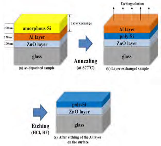
Schematic drawing of the fabrication process of poly-Si layer by the ZnO-assisted aluminum-induced layer exchange process: (a) amorphous Si/Al/ZnO/glass stacked sample (as-deposited sample); (b) Al/poly-Si/ZnO/glass stacked sample (layer exchanged sample); (c) poly Si/ZnO/glass (after etching of the Al layer on the surface).
The surface roughness of the ZnO layer was evaluated by atomic force microscopy (AFM, Park systems XE-100). The morphological change of the poly-Si films during annealing was monitored in situ by optical microscopy. The sample surface was observed using Scanning electron microscopy (SEM; JEOL JSM-7000F). The sample surface was polished with a cross section polisher, and it was subjected to crosssectional SEM analysis. Energy-dispersive spectroscopy (EDS) was conducted to analyze the elemental distribution in the samples. Electron backscatter diffraction (EBSD) was performed to evaluate the orientation of grains; the results obtained were as follows: the average misorientation angle between the grains was approximately 6° and the electron beam incident angle was 70°, at an acceleration voltage of 20 kV. The beam spot size was 5.4 μm and the step size was 0.2 μm.
3. Results and discussion
Figure 2 shows the AFM images of the ZnO layer surface. The root mean square (RMS) roughness of the ZnO layer was controlled by changing the oxygen flow during the deposition. The corresponding RMS roughness of the ZnO layer was a) 0.73 nm (O2 flow = 0 sccm, Pchamber = 3 × 10⁻³ Torr); b) 1.42 nm (O2 flow = 8 sccm, Pchamber = 5 × 10⁻³ Torr), and c) 2.4 nm (O2 flow = 10 sccm, Pchamber = 6 × 10⁻³ Torr). As shown in the inset of Figure 2, all samples were transparent. Previous studies have shown that an excess of oxygen increases the surface roughness of ZnO layer by restricting the surface migration length[15].
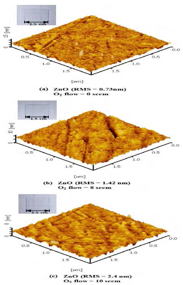
AFM images of the ZnO layers grown on glass substrates: (a) ZnO/glass (RMS: 0.73 nm); (b) ZnO/glass (RMS: 1.43 nm); (a) ZnO/glass (RMS: 2.4 nm). The insets in the upper-left corner show pictures of each sample.
Using the aforementioned ZnO-coated substrates with varying ZnO layer surface roughness, thermal deposition of Al, deposition of α-Si by sputtering, and the layer exchange process were accomplished sequentially under the same experimental conditions. Three samples were prepared. Samples A, B, and C were prepared on ZnO layers with surface roughnesses of 0.73 nm, 1.42 nm, and 2.4 nm, respectively. The samples were simultaneously annealed at 577 °C.
Schematic of the ALE process is shown in Figure 3. It shows the cross-sectional SEM (left-hand side) and corresponding EDS maps (right-hand side) of the as-deposited sample (Figure 3(a)) and the annealed sample (Figure 3(b)). Figure 3(a) shows the α- Si/Al/ZnO/glass stack, while Figure 3 (b) shows an Al/poly- Si/ZnO/glass stack. The layer-exchange process can be explained as follows: at the eutectic temperature of 577 °C, the Si (12.7 %)- Al(87.3 %) alloy begins to melt and Si nuclei form in the Al layer [6][16]. As the melting continues, Si nuclei merge to form a poly-Si layer [11]. The nucleation speed (i.e., growth rate) is affected by various parameters, such as temperature, dissolution flux, and mobility of Si in the Al layer. At a given temperature, the dissolution flux is determined by the concentration of the Al–Si alloy. Ideally, a smooth, abrupt interface between the Al and Si layers will support uniform dissolution flux across the entire interface; a rough interface will induce spatial concentration fluctuations in the dissolution flux.
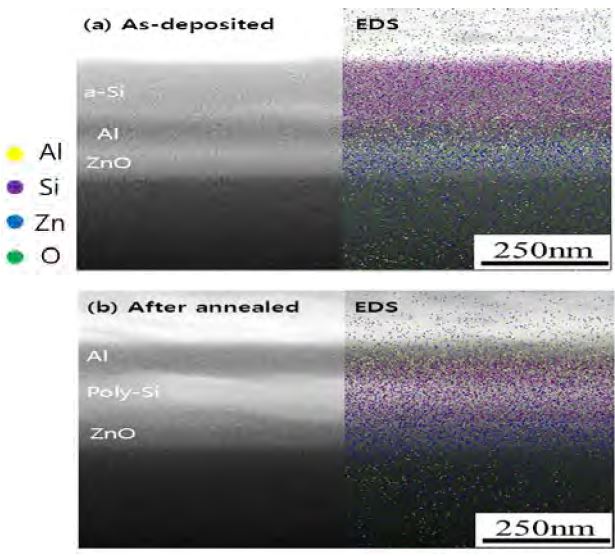
Cross-sectional SEM images (left) and EDS mapping images (right): (a) as-deposited sample with a stacking sequence of α- Si/Al/ZnO/glass and (b) annealed (577 °C) sample, which has a stacking sequence of Al/poly Si/ZnO/glass.
The crystallization process of the poly-Si layer was observed during annealing. Figure 4 shows optical microscopy images, as seen from the underside, through the quartz substrate. The images of the samples were featureless at the beginning (0 min). In the case of Sample A, low-density, small-size nuclei emerged after 30 min of annealing, and dendritic growth followed, implying a very low growth rate[17]-[20]. In the case of the other two samples, the nuclei emerged much earlier (after ~15 min for Sample B and ~10 min for Sample C), and grew faster as well. The fact that dendritic growth did not occur in the case of Samples B and C indicates an increase in the growth rate. The high growth rate could be attributed to an increase in the amount of the Si dissolution, as the annealing temperature was the same for all samples.
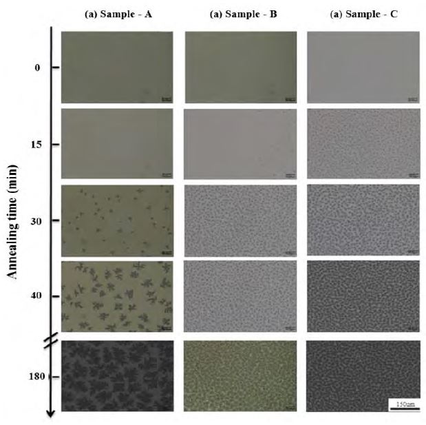
Optical micrographs obtained during the layer exchange process: (a) Sample A, (b) Sample B, and (c) Sample C. The black areas in the picture correspond to the poly-Si nuclei.
Here it would be appropriate to discuss, in detail, the correlation between the surface roughness of the ZnO layer and the growth rate. There have been several reports on the correlation between the Aloxide membrane and the growth of Si-nuclei. Klein et al. reported on the increase in growth rate with low quality Al-oxide membranes[21]. Furthermore, Kim et al. [9] carried out the ALE process with and without the Al-oxide membrane. With the Al-oxide membrane, they observed a higher growth rate. On the other hand, without the Aloxide membrane, but a poly Si layer was not obtained. Therefore, a possible explanation for the results in Figure 4 is that the surface roughness of the ZnO layer affects the dissolution flux of Si by changing the structural quality of the Al-oxide membrane.
Figure 5 shows the variation in the crystallization fraction (CF) as a function of annealing time, showing the growth rate of the Si grains, quantitatively. The CF was quantified from the optical microscope images (Figure 4). Sample A revealed ~62% of CF (~20 min), while Sample B showed ~65% of CF (~60 min). The largest CF (~84%), was achieved in the shortest time (~40 min), for Sample C. Note that the reported CF values were in the range of 80–90%, in results of annealed for a few hours or for a few weeks [22]-[24].
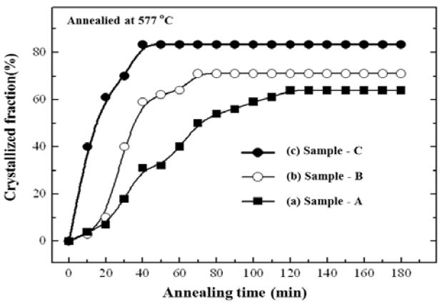
Annealing time dependency of the crystallization fraction. The crystallization rate of poly-Si is closely related to the roughness of the ZnO layer.
Figure 6 shows the in-plane EBSD images. The black area represents α-Si, and the colored area represents poly-Si clusters. The crystallized area increased with the surface roughness of the ZnO layer. In addition, preferential orientation of the grains is found to be along the Si (100) direction. Note that as the crystallization fraction increases (i.e., as the growth rate increases), more clusters tend to be aligned in the Si (100) direction.
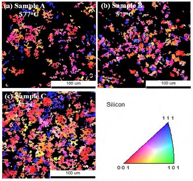
In-plane EBSD images of (a) Sample A, (b) Sample B, and (c) Sample C. One can observe that the preferential orientation of poly-Si is closely related to the surface roughness of the ZnO layer.
The effect of crystallization conditions, such as substrate and temperature, on the preferential orientation of poly-Si has attracted a lot of attention. In case of dependence on the substrate, a preferential Si (111) orientation was observed on glass substrate [25], while a preferential Si (100) orientation was observed for growth on ZnO surface [26]. Oxidation of the Al layer prior to the deposition of the α-Si is known to be helpful in obtaining Si (100) orientation. Schneider et al. [26] have reported that the nucleation rate of clusters with an orientation close to the Si (100) direction is higher that of clusters with other orientations, due to the higher surface energy of the Si (100) plane. Therefore, we conclude that a high growth rate is responsible for the preferential Si (100) orientation of the clusters.
4. Summary and Conclusion
This study investigated the influence of the surface roughness of the ZnO layer on the ALE growth of poly-Si layer. It was found that both the growth rate and the preferential orientation are closely related to the surface roughness of the underlying ZnO layer. As the ZnO surface roughness increases, a higher growth rate due to spatial fluctuation of the dissolution flux was observed. This induces the preferential Si (100) orientation that is essential for the fabrication of a poly-Si thin film solar cell.
Acknowledgments
This research was supported by the International Research & Development Program of the National Research Foundation of Korea (NRF) funded by the Ministry of Education, Science and Technology (MEST) of Korea (Grant number: D00013).
References
-
S. D. Brotherton, J. R. Ayres, and N. D. Young, “Characterisation of low temperature poly-Si thin film transistors”, Solid-State Electronics, 34(7), p671-679, (1991).
[https://doi.org/10.1016/0038-1101(91)90002-G]

-
O. Nast, T. Puzzer, L. M. Koschier, A. B. Sproul, and S. R. Wenham, “Aluminum-induced crystallization of amorphous silicon on glass substrates above and below the eutectic temperature”, Applied Physics Letters, 73(22), p3214-3216, (1998).
[https://doi.org/10.1063/1.122722]

-
Y. Matsumoto, and Z. P-type, “Polycrystalline Si Films Prepared by Aluminum-Induced Crystallization and Doping Method”, Japanese Journal of Applied Physics, 40, 40(4A), p2110-2114, (2001).
[https://doi.org/10.1143/JJAP.40.2110]

-
B. Rau, I. Sieber, J. Schneider, M. Muske, M. Stőger-Pollach, P. Schattschneider, S. Gall, and W. Fuhs, “Lowtemperature Si epitaxy on large-grained polycrystalline seed layers by electron–cyclotron resonance chemical vapor deposition”, Journal of Crystal Growth, 270(3-4), p396-401, (2004).
[https://doi.org/10.1016/j.jcrysgro.2004.07.034]

-
D. Van Gestel, I. Gordon, L. Carnel, K. Van Nieuwenhuysen, J. D´Haen, J. Irigoyen, G. Beaucarne, and J. Poortmans, “Influence of seed layer morphology on the epitaxial growth of polycrystalline-silicon solar cells”, Thin Solid Films, 511-512, p35-40, (2006).
[https://doi.org/10.1016/j.tsf.2005.12.149]

-
J. Schneider, J. Klein, M. Muske, S. Gall, and W. Fuhs, “Depletion regions in the aluminum-induced layer exchange process crystallizing amorphous Si”, Applied Physics Letters, 87, p031905, (2005).
[https://doi.org/10.1063/1.1996849]

-
H. Kuraseko, N. Orita, H. Koaizawa, and M. Kondo, “Inverted Aluminum-Induced Layer Exchange Method for Thin Film Polycrystalline Silicon Solar Cells on Insulating Substrates”, Applied Physics Express, 2(1), p015501, (2009).
[https://doi.org/10.1143/APEX.2.015501]

- D. Dimova-Malinovska, O. Angelov, M. Kamenova, A. Vaseashta, and J. C. Pivin, “Structural properties of poly- Si thin films grown on ZnO: Al coated glass substrates by aluminum induced crystallisation”, Journal of optoelectronics and advanced materials, 9(2), p355-358, (2007).
-
H. Kim, D. Kim, G. Lee, D. Kim, and S. H. Lee, “Polycrystalline Si films formed by Al-induced crystallization (AIC) with and without Al oxides at Al/a- Si interface”, Solar Energy Materials and Solar Cells, 74(1-4), p323-329, (2002).
[https://doi.org/10.1016/S0927-0248(02)00091-0]

-
G. Willeke, H. Nussbaumer, H. Bender, and E. Bucher, “A simple and effective light trapping technique for polycrystalline silicon solar cells”, Solar Energy Materials and Solar Cells, 26(4), p345-356, (1992).
[https://doi.org/10.1016/0927-0248(92)90054-S]

-
D. Tsukada, Y. Matsumoto, R. Sasaki, M. Takeishi, T. Saito, N. Usami, and T. Suemasu, “Fabrication of (111)- oriented Si layers on SiO2 substrates by an aluminuminduced crystallization method and subsequent growth of semiconducting BaSi2 layers for photovoltaic application”, Journal of Crystal Growth, 311, p3581-3586, (2009).
[https://doi.org/10.1016/j.jcrysgro.2009.04.039]

-
J. Muller, B. Rech, J. Springer, and M. Vanecek, “TCO and light trapping in silicon thin film solar cells”, Solar Energy, 77(6), p917-930, (2004).
[https://doi.org/10.1016/j.solener.2004.03.015]

-
O. Kluth, G. Schöpe, J. Hüpkes, C. Agashe, J. Mueller, and B. Rech, “Modified Thornton model for magnetron sputtered zinc oxide: film structure and etching behavior”, Thin Solid Films, 442, p80-85, (2003).
[https://doi.org/10.1016/S0040-6090(03)00949-0]

-
B. Rech, T. Repmann, M. N. van den Donker, M. Berginski, T. Kilper, J. Hűpkes, S. Calnan, H. Stiebig, and S. Wieder, “Challenges in microcrystalline silicon based solar cell technology”, Thin Solid Films, 511-512, p548-555, (2006).
[https://doi.org/10.1016/j.tsf.2005.12.161]

-
C. Y. Ma, F. Lapostolle, P. Briois, and Q. Y. Zhang, “Effect of O2 gas partial pressure on structures and dielectric characteristics of rf sputtered ZrO2 thin films”, Applied Surface Science, 253(21), p8718-8724, (2007).
[https://doi.org/10.1016/j.apsusc.2007.04.054]

-
J. Schneider, A. Schneider, A. Sarikov, J. Klein, M. Muske, S. Gall, and W. Fuhs, “Aluminum-induced crystallization: nucleation and growth process”, Journal of Non-Crystalline Solids, 352(9-20), p972-975, (2006).
[https://doi.org/10.1016/j.jnoncrysol.2005.09.036]

-
C. W. Lan, C. M. Hsu, C. C. Liu, and Y. C. Chang, “Adaptive phase field simulation of dendritic growth in a forced flow at various supercoolings”, Physical Review E, 65, p061601, (2002).
[https://doi.org/10.1103/PhysRevE.65.061601]

-
C. W. Lan, C. M. Hsu, and C. C. Liu, “Efficient adaptive phase field simulation of dendritic growth in a forced flow at low supercooling”, Journal of Crystal Growth, 241, p379-386, (2002).
[https://doi.org/10.1016/S0022-0248(02)01287-3]

-
N. Provatas, N. Goldenfield, and J. Dantzig, “Efficient computation of dendritic microstructures using adaptive mesh refinement”, Physical Review Letters, 80, p3308-3311, (1998).
[https://doi.org/10.1103/PhysRevLett.80.3308]

-
H. K. Lin, C. C. Chen, and C. W. Lan, “A simple anisotropic surface free energy function for threedimensional phase field modeling of multi-crystalline crystal growth”, Journal of Crystal Growth, 362, p62-65, (2013).
[https://doi.org/10.1016/j.jcrysgro.2012.01.004]

-
J. Klein, J. Schneider, M. Muske, S. Gall, and W. Fuhs, “Aluminium-induced crystallisation of amorphous silicon: influence of the aluminum layer on the process”, Thin Solid Films, 451-452, p481-484, (2004).
[https://doi.org/10.1016/j.tsf.2003.11.009]

-
M. N. Jung, A. Okada, T. Saito, T. Suemasu, and N. Usami, “On the Controlling Mechanism of Preferential Orientation of Polycrystalline-Silicon Thin Films Grown by Aluminum-Induced Crystallization”, Applied Physics Express, 3(9), p095803, (2010).
[https://doi.org/10.1143/APEX.3.095803]

-
K. Y. Lee, M. Muske, I. Gordon, M. Berginski, J. D’Haen, J. Hupkes, S. Gall, and B. Rech, “Large-grained poly-Si films on ZnO:Al coated glass substrates”, Thin Solid Film, 516, p6869-6872, (2008).
[https://doi.org/10.1016/j.tsf.2007.12.128]

-
G. Ekanayake, T. Quinn, and H. S. Reehal, “Largegrained poly-silicon thin films by aluminum-induced crystallisation of microcrystalline silicon”, Journal of Crystal Growth, 293, p351-358, (2006).
[https://doi.org/10.1016/j.jcrysgro.2006.05.083]

-
Y. Sugimoto, N. Takata, T. Hirota, K. Ikeda, F. Yoshida, H. Nakashima, and H. Nakashima, “Low-temperature fabrication of polycrystalline Si thin film using Alinduced crystallization without native Al Oxide at amorphous Si/Al interface”, Japanese Journal of Applied Physics, 44, p4770-4775, (2005).
[https://doi.org/10.1143/JJAP.44.4770]

-
J. Schneider, A. Sarikov, J. Klein, M. Muske, I. Sieber, T. Quinn, H. S. Reehal, S. Gall, and W. Fuhs, “A simple model explaining the preferential (1 0 0) orientation of silicon thin films made by aluminum-induced layer exchange”, Journal of Crystal Growth, 287, p423-427, (2006).
[https://doi.org/10.1016/j.jcrysgro.2005.11.057]
