Analysis of nano-cluster formation in the PECVD process
In this paper, the ultra water-repellent thin films were prepared by RF PECVD. On the basis of surface morphology, chemical bonding states and plasma diagnostics, a formation model of clusters for the ultra water-repellent films was discussed from considerations of formation process and laser scattering results. Moreover, using laser scattering method, the relative change of quantity of nano-clusters or size of agglomerates could be confirmed. From the results, the films were deposited with nano-clusters and those of agglomerates, which formed in organosilicon plasma, and formation of agglomerates were depended on the deposition time.
Keywords:
Ultra water repellen thin films, SiO:CH, OES, Nano cluster, PECVD1. Introduction
Water repellent (WR) phenomenon is important from both academic and industrial applications. It has been studied since Young’s paper in 1805 and accumulated in many aspects[1]-[3]. In particular, ultra water- repellent (UWR) films, with a water contact angle greater than 150°, have been researched by many techniques, such as CVD, sol-gel and nano-imprinting method, etc.[3]-[7]. Conventionally, the water repellency can be enhanced in two ways; one is a change of chemical functional group with low surface energy, leading to the order of 100 to 120 degree. The other is an improvement of surface roughness to increase the specific surface area resulting in an increase of nominal surface energy. For the formation of UWR films, a modification of surface chemistry is always combined with a surface roughness enhancement[8][9].
We have succeeded in fabricating UWR thin films at room temperature by plasma-enhanced chemical vapor deposition (PECVD)[6][7]. However,the formation mechanism of clusters in the PECVD process has not been clarified. In this study, we investigated the clustering phenomena by deducing from results of surface morphology, water contact angle of the films and laser scattering in Ar-organosilicon plasma.
2. Experimental procedure
This work was carried out with a ICP rf PECVD system[7]. The PECVD system consists of deposition chamber and aquartz discharge tube whose length and diameter was 200 and 55mm, respectively, coupled with a copper rf coil. A 13.56 MHz generator (ENI, OEM-12A) supplied the RF power into the copper. The reactant used in this work was trimethylmethoxysilane (TMMOS; (CH3)3SiOCH3). N-type Si (100) substrate was located at 200 mm below from the center of the plasma to avoid direct thermal damage by the plasma. In order to regulate a total gas flow rate, firstly argon gas was introduced into the chamber with a constant flow rate of 10 sccm when its pressure was fixed at 80 Pa by controlling vacuuming rate. Secondly, the reactant gas of TMMOS was introduced up to 500 Pa. After the deposition, water repellency of the films was measured by static water contact angle meter (Kruss, DSA10-Mk2). The surface morphology was observed by a field emission scanning electron microscope (FESEM; JEOL, JSM-6330F). Plasma diagnostics was performed by optical plasma emission spectroscopy (OES, Chromex, 500-IS).
3. Results and discussion
To deposit the UWR films, it is important two points; one is an introduced energy to dissociate and recombine the reactant, and the other is a mean residence time of precursors to generate the cluster in the plasma. In the previous work[7],the UWR films could be fabricated reproducibly at 500 Pa of pressure. Even though a mean residence time has become not significant due to a saturated exhaust speed in the high pressure region, a few seconds of mean residence time of precursors is necessary to form the sufficient surface roughness for the UWR films.
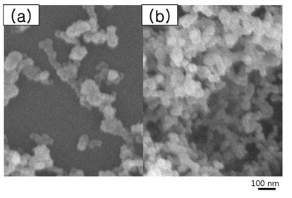
About the introduced energy, the water contact angle was increased with RF power. And the UWR surfaces could be fabricated at above 150 W of rf power. Figure 1 shows SEM images of the UWR films, which were deposited at ~ 100 - 150 W of rf power. In all conditions, we can observe the nano-clusters of several tens of nm. In 100 W of rf power, the surface morphology of thin films was close to flat even though the clusters existed, which led to WR property. In 150 W, the film had micrometer size pores in a self-assembled cancellous microstructure, which consists of nano-size globular clusters, resulted in the UWR film.
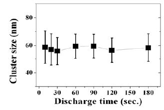
To investigate the growth process of the clusters, the cluster size distribution with deposition time was shown in Figure 2. On the whole, the size distribution was not altered under different deposition time. This result suggests that the nano-clusters are possible to grow up the specific space in the chamber independent of deposition time. Regarding this phenomena, however, it calls for further investigation.
In the previous investigation of surface morphology with deposition time, before 20 seconds of deposition time, even before 10 seconds, single nano-clusters were observed primarily. The films deposited after the 20 seconds, on the other hand, agglomerated clusters composed of single nano-clusters were observed [7].These results suggest that the nano-clusters were agglomerated in the plasma with the deposition time. From above results, it is important following two conditions in clustering phenomena in the plasma. One is an introduced energy to promote dissociation and recombination reactions. In this work, the UWR films could be fabricated reproducibly at the pressure condition of 500 Pa. The other is a mean residence time of precursors to generate the cluster in the plasma. That is, it is necessary the specific mean residence time to transfer the rf energy for dissociation and recombination reaction in plasma. In this work, at least approximately 1.15 sec. of actual mean residence time of precursors is necessary to form the clusters in organosilicon plasma. The 1.15 sec. of mean residence time of precursors in the chamber, calculated from the volume of chamber / the exhaust velocity in this study. However, the conductance of the vacuum line in the system is not considered in the above estimation.
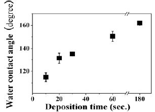
Figure 3 indicates a water contact angle of the films deposited at different deposition time of ~ 10 - 180 seconds. The water contact angle was increased with deposition time. In 10 seconds of deposition time, the water contact angle of the films was approximately 115 degree, caused by the relatively smooth surface terminated by CH3 hydrophobic functional group from TMMOS reactant. In 20 ~ 30 seconds of deposition time, the water contact angle was elevated than those of 10 seconds due to an enhancement of surface roughness by the nano-clusters. The geometrical effect for these surfaces is ascribable to the expansion of the nominal surface area (Wenzel-style effect). In 60 seconds, the rough surfaces of the films result in over 150 degree of the water contact angle. The water contact angle of the films was increased slightly until 162 degree for 180 seconds. In this regime, the geometrical effect of the air trapping between a water-droplet and textures on the film surface, which minimizes the contact area can be caused (Cassie-style effect)[8][9].
For the clustering phenomena or polymerization - like reactions in gas phase, laser scattering system was prepared. 532 nm DPSS laser introduced to a chamber window, and scattered laser was detected by the same system for OES. Intensity of scattered laser was obtained for 3 sec. later from plasma turned off.
Figure 4 shows the images of scattered laser by clusters formed in organosilicon plasma. Under the 500 Pa of pressure and 150 W of rf power, which is the deposition condition for the UWR films, scattered light was observed at turning off plasma. These results signify the existence of nano-clusters in organosilicon plasma, supporting that the UWR films were deposited with nano-clusters formed in plasma. From a relation between the average size of nano-clusters (58.3±10.1 nm, deposition condition of 500 Pa, 150 W) and the wavelength of DPSS laser was 532 nm, it can be said that scattered light by the single nano-clusters originated by Rayleigh scattering phenomenon. In the case of agglomerates, those of sizes were over 500 nm, i.e. scattering phenomenon is possible to transfer from Rayleigh to Mie scattering. In the Mie scattering regime, complicated patterns of scattered light revealed due to forward scattered light by large cluster size. In this work, however, dependence of scattered angle cannot be expected due to a random distribution of low dense and non-spherical agglomerates in the plasma.
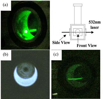
Images of scattered laser by clusters formed in organosilicon plasma ((a): side view, (b): front view, plasma on and (c): front view, plasma off)
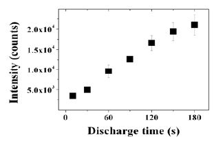
Figure 5 shows the time dependence on intensity of scattered laser by clusters formed in organosilicon plasma. Scattered laser intensity increased linearly with the deposition time. The intensity of scattered laser consists of an ingredient of Rayleigh scattered light by single nano-clusters and one of Mie scattered light by agglomerates. Regarding the Rayleigh scattered light, it can be said that the scattered intensity of 10 sec. is originated only by Rayleigh scattering phenomenon of single nano-clusters, and one of other discharge time condition includes a similar or less amount of Rayleigh scattered light. Concerning the increase of scattered light, this is included the meaning of an increase of amount of nano-clusters or agglomerates, and an enlargement of agglomerates.
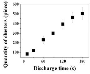
Regarding the scattered laser intensity, several analyses were performed by some assumptions. Firstly, Figure 6 shows the time dependence on amounts of nano-clusters calculated from the intensity of scattered laser (Figure 5) and SEM image[11]. This graph was plotted from the following procedure: 1. Nano-clusters were formed 83 pieces during 10 sec.. 2. Scattered laser intensity at 10 sec. is equivalent to 83 pieces of the nano-clusters. This calculation was performed by a hypothetical condition of Rayleigh scattering agglomerates, With this model, it is convenient to analyze the aspect of clustering process in the organosilicon plasma, because a size of agglomerates can be included in a quantity of nano-clusters. However, it is necessary to confirm the scattering phenomenon of complicated shape of scattering centers. From the result of calculation, quantity of nano-clusters increased with deposition time, and increase of nano-clusters seem to be saturated slightly at approximately 500 pieces.
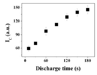
In order to indicate a size of agglomerates in the organosilicon plasma, the square root of scattered laser intensity (IC) was plotted in Figure 7. In spite of this too simple model, it can be an excellent reference data to clarify the deposition process. That is, IC increased with deposition time, and saturated slightly near 150 sec. Moreover, in 60 sec, increment of IC accelerated comparing with one of below 60 sec. These analyses could be corresponded with previous results in time dependant deposition of UWR films [11].
4. Summary
From the above consideration on the plasma reactions, the formation mechanism of clusters as follows; 1. TMMOS reactant is partly dissociated by RF power. 2. The dissociated TMMOS precursors are recombined to grow up the single clusters in the plasma independent of deposition time. 3. The single clusters are agglomerated in the plasma or film surface.
References
-
H. M. Shang, Y. Wang, S. J. Limmer, T. P. Chou, K. Takahashi, and G. Z. Cao, "Optically transparent superhydrophobic silica-based films", Thin Solid Films, 472, p37, (2005).
[https://doi.org/10.1016/j.tsf.2004.06.087]

-
X. Lu, C. Zhang, and Y. Han, "Low-density polyethylene superhydrophobic surface by control of its crystallization behavior", Macromolecular Rapid Communications, 25, p1606, (2004).
[https://doi.org/10.1002/marc.200400256]

-
W. Li, and A. Amirfazli, "A thermodynamic approach for determining the contact angle hysteresis for superhydrophobic surfaces", Journal of Colloid and Interface Science, 292, p195-201, (2005).
[https://doi.org/10.1016/j.jcis.2005.05.062]

-
H. Y. Erbil, A. L. Demirel, Y. Avci, and O. Mert, "Transformation of a simple plastic into a superhydrophobic surface”, Science, 299, p1377-1380, (2003).
[https://doi.org/10.1126/science.1078365]

-
A. Nakazima, A. Fuzishima, K. Hashimoto, and T. Watanabe, "Preparation of transparent superhydrophobic boehmite and silica films by sublimation of aluminum acetyl acetonate", Advanced Materials, 11, p1365-1368, (1999).
[https://doi.org/10.1002/(SICI)1521-4095(199911)11:16<1365::AID-ADMA1365>3.3.CO;2-6]

-
Y. Wu, M. Kuroda, H. Sugimura, Y. Inoue, and O. Takai, "Nanotextures fabricated by microwave plasma CVD: application to ultra water-repellent surface", Surface and Coating Technology, 174-175, p867-871, (2003).
[https://doi.org/10.1016/S0257-8972(03)00420-1]

-
Y. Yun, "Formation of SiO:CH ultra water repellent thin films by inductively coupled RF PECVD", Journal of Korean Society of Marine Engineering, 35, p323-328, (2011).
[https://doi.org/10.5916/jkosme.2011.35.3.323]

-
Z. Yoshimitsu, A. Nakajima, T. Watanabe, and K. Hashimoto, "Effects of surface structure on the hydrophobicity and sliding behavior of water droplets", Langmuire, 18, p5818-5822, (2002).
[https://doi.org/10.1021/la020088p]

-
A. Lafuma, and D. Quere, "Superhydrophobic states", Nature Materials, 2, p457, (2003).
[https://doi.org/10.1038/nmat924]

-
Y. Yun, T. Yoshida, N. Shimazu, Y. Inoue, N. Saito, and O. Takai, "Behavior of various organosilicon molecules in PECVD processes for hydrocarbon - doped silicon oxide films", Solid State Phenomena, 124-126, p347-350, (2007).
[https://doi.org/10.4028/www.scientific.net/SSP.124-126.347]

-
Y. S. Yun, T. Yoshida, N. Shimazu, N. Nanba, Y. Inoue, N. Saito, and O. Takai, "Fabrication of ultra water-repellent thin films by PECVD method and observation of deposition process", Journal of The Surface Finishing Society of Japan, 58, p307-311, (2007).
[https://doi.org/10.4139/sfj.58.307]

