Micropatterning of self-assembled monolayers using vacuum ultraviolet light
Copyright ⓒ The Korean Society of Marine Engineering
This is an Open Access article distributed under the terms of the Creative Commons Attribution Non-Commercial License (http://creativecommons.org/licenses/by-nc/3.0), which permits unrestricted non-commercial use, distribution, and reproduction in any medium, provided the original work is properly cited.
Abstract
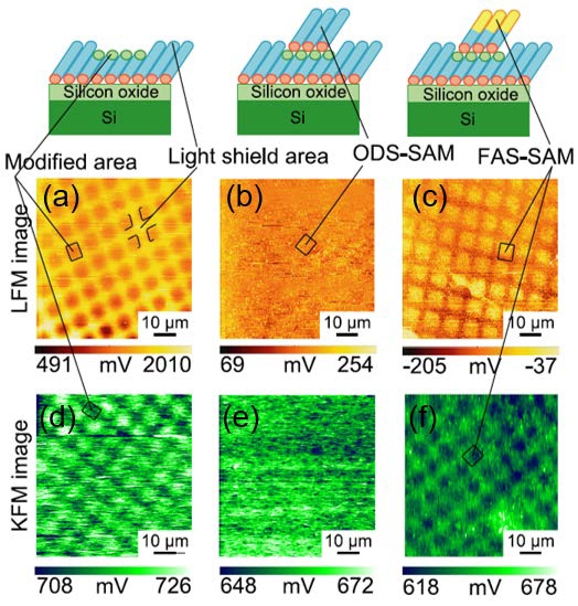
A micropatterning technique was applied to an n-octadecyltrimethoxysilane self-assembled monolayer (ODS-SAM) formed on Si substrates covered with a 2 nm thick layer oxide using excimer lamps to radiate vacuum ultraviolet (VUV) light at 172 nm in wavelength. The results of Kelvin-probe force microscopy (KFM) and lateral force microscopy (LFM) analyses showed that the second monolayer was stacked to the VUV-modified area of the ODS-SAM. Oxides, i.e., –COOH groups, were formed before the ODS-SAM completely decomposed and was removed from the substrate. Coplanar binary alkylsilane SAM microstructures were successfully fabricated by adopting the response between –OCH3 functional groups with –COOH groups on the ODS-SAM modified using VUV light. Furthermore, as shown in the KFM image, the region covered with the FAS had a surface potential ~60 mV lower than that of the region covered with ODS. The origin of the image contrasts between the ODS- and FAS-SAMs was the significant difference in the electronic states between the ODS and FAS owing to the electron negativity of fluorine atoms. The difference in the surface chemical composition of the SAMs could be clearly and sensitively measured through KFM based on the difference in the surface potential between the ODS and FAS.
Keywords:
Self-assembled monolayer, Vacuum ultraviolet light, Micropatterning, Microstructure, Kelvin-probe force microscopy, Lateral force microscopy1. Introduction
In recent years, interest in the fabrication of microstructures composed of organic molecules in artificial design is increasing in the marine, microelectronics, and biotechnology industries. Furthermore, marine-textured antifouling coatings are actively being developed using the micropatterning technique [1]. Oxides are the main compounds in microelectronic components that are widely used in insulators [2], piezoelectric [3], ferroelectronics [4], and ferromagnetics [5]. However, because of its extended chemical durability and physical stability to electron beams and lasers, it is difficult to micropattern oxides through typical microfabrication processing using chemical or physical etching methods. Consequently, their microprocessing is currently achieved through complicated photolithographic technology involving several processes. Therefore, an alternative method requiring neither etching nor additional posttreatment methods is necessitated.
An approach involves using patterned organosilane self-assembled monolayers (SAMs). SAMs can be applied in various areas. It is believed that SAMs can be applied to the corrosion protection of electronic devices and precision circuit components in the marine industry under harsh environmental conditions [6]. Organosilane SAMs have been frequently used as patternable materials in microfabrication processes [7]. Because this technique is the most feasible owing to its ability to transfer the entire pattern of the photomask to a SAM through a single exposure, photolithography methods have been generally adopted for organic SAMs prepared homogeneously via micro-patterns. However, the photolysis mechanism has not been investigated in detail, although knowledge of this mechanism can be useful in the optimization of the SAM micropatterning process. Most previous studies were focused on the primary photolysis pathway of alkylsilanes or alkanethiol SAMs to ozonolysis [8]. In addition, some researchers concluded that the combination of ultraviolet (UV) radiation [9] and oxygen is necessary for the degradation of alkylsiloxane SAM [10]. However, the condition of the irradiated SAMs remaining on the substrate during the photolysis process has not been discussed in detail.
As the carboxyl-terminated surface is relevant in the micro/nanofabrication processes, in this study, the alkylsilane SAM, i.e., octadecyltrimethoxysilane SAM, was terminated with a carboxyl group [11]. Furthermore, this method was applied to the formation of binary organic microstructures consisting of n-octadecyltrimethoxysilane (ODS) and fluoroalkylsilane (FAS) molecules.
2. Experimental method
2. 1 Sample
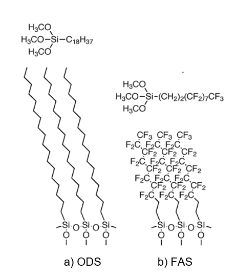
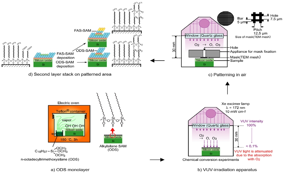
Two types of organosilane precursors, i.e., ODS [CH3(CH2)17Si(OCH3)3] and FAS [heptadecafluoro-1,1,2,2-tetrahydrodecyl-1-trimethoxysilane; [F3C(CF2)7(CH2)2Si(OCH3)3] were obtained from Gelest Inc. and used as received for SAMs. The chemical formulas of these precursors and their corresponding SAMs are shown in Figure 1. ODS-SAM was prepared on a Si (100) substrate covered with a natural thin oxide layer (ca. 2 nm) using a chemical vapor deposition (CVD) method [12]. The samples were produced using the procedure schematically illustrated in Figure 2.
First, all the substrates cut from the wafer were washed with ethanol and ultrapure water for 20 min in this order. Next, the washed substrates were photochemically cleaned and hydroxylated simultaneously through vacuum UV (VUV) generated using an excimer lamp (Ushio. Inc., UER20-172V; intensity at lamp window of 10 mW cm-2) for 20 min at a lamp–sample distance of 5 mm in air. This photochemical washing method is described in the literature [12].
In a nitrogen-filled glove at a regulated humidity of approximately 17%, the sample and 60 μL of ODS liquid in a 3 cm3 glass cup were placed in a 120 cm3 Teflon container. The container was then sealed using a screw cap and placed in an electric oven at 150 °C for 3 h. The ODS liquid in the vessel vaporized and reacted with –OH groups on the silicon sample surfaces. The molecules were fixed onto the sample surfaces and connected to adjacent ODS molecules via siloxane bonds (Figure 2 a). The increase in the contact angle from 0° to 104° on the average indicated the formation of ODS-SAM, and the estimated thickness of the ellipsometry was approximately 1.4–1.5 nm using the air/SiO2/Si model. The specific properties of the vapor-phase-grown ODS-SAMs have been reported [13].
Second, photolithography micropatterning was performed on the samples covered with ODS-SAM (Figure 2 b,c). The ODS-SAM surface was locally irradiated through a photomask for 40 min at a lamp–sample distance of 30 mm using VUV light. Based on the results of our previous study [13], we reflected the optimization conditions for the chemical conversion of this VUV light system. Finally, in the micropatterned ODS-SAM sample used as a template for the second CVD, FAS or ODS was selectively stacked in the VUV-modified region of the ODS-SAM. Thus, the binary microstructures composed of ODS/FAS and ODS/ODS were fabricated by selectively stacking two SAMs, i.e., FAS or ODS molecules, into a VUV-modified region (Figure 2 d).
2. 2 Characterization
The samples were analyzed through Kelvin-probe force microscopy (KFM) and lateral force microscopy (LFM) using a scanning probe microscope (SPM, Seiko Instruments Inc., SPA-300HV + SPI3800N), and the microscope was set in a vacuum chamber. Air was released until the pressure in the chamber was less than 10-4 Pa to minimize the effects of the adsorbed water on the sample. The chamber was then filled with nitrogen. KFM was performed in this nitrogen atmosphere using a gold-coated Si cantilever with a force constant of approximately 2 N m-1, resonance frequency of approximately 30 kHz, and Q factor of approximately 180. Non-contact atomic force microscopy was performed during KFM imaging based on the amplitude detection mode. The cantilever vibrated at a slightly lower frequency than the resonance frequency. While the conductive cantilever was grounded, an alternating-current voltage of 2 V at frequency 2–3 kHz lower than the cantilever vibration frequency was applied to the sample. The KFM images of the sample surfaces were captured at a probe scan rate of 0.1–0.2 Hz. The LFM images of the samples were acquired in a nitrogen atmosphere under a load of 10 nN using an Si probe (Park Scientific Instruments, Ultralever, force constant = 2.8 N m-1). The same probe was used in this study to minimize the differences in the contact area between each measurement and to compare the measured lateral forces accurately.
3. Results and discussion
Before we explain the steps of obtaining the second layer stack, first, we discuss the VUV photolysis mechanism of ODS-SAMs. Several reports of photochemical reactions from chloromethylphenylsilane SAM to COOH-terminated SAMs exist [11]. In this case, the –CH2Cl groups absorbed UV light and subsequently oxidized it with oxygen.
However, in the case of the VUV decomposition of ODS-SAMs, the VUV light separates chemical bonds and forms radicals [14], such as C–C, C–H, and C–Si, during soft X-ray irradiation. [15]. These radicals can react more with atmospheric oxygen and water molecules. Because the VUV irradiation for ODS-SAMs was performed in air, this reaction was more efficient in our study because more than 1000 times of oxygen molecules were formed on the sample surface than in previous studies conducted in vacuum [16]. Moreover, the VUV light was absorbed simultaneously with the oxygen molecules, producing atomic oxygen species [17]. Because these reactive oxy-gen atoms exhibited strong oxidation reactivity, the organic radicals formed through direct VUV stimulation of ODS-SAMs reacted further with activated oxygen atoms to form –COOH groups. As VUV irradiation became prolonged, the ODS-SAM was finally converted to volatile species, such as H2O, CO, and CO2, and removed from the substrate.
Next, the second SAM, i.e., FAS or ODS, was deposited onto the ODS-SAM/Si substrate micropatterned with VUV irradiation for 40 min through a photomask at a lamp-sample distance of 30 mm. During this irradiation, it was assumed that the VUV-radiation region of the ODS-SAM was covered with the –COOH group, as observed in previous studies [13].
The LFM and KFM images of the micropatterned ODS (a, d), ODS second layer stack (b, e), and FAS second layer stack (c, f) samples are depicted in Figure 3. The ODS-covered region had a surface potential 18 mV lower than that for the COOH-exposed region (Figure 3 d). Figure 3 c shows an LFM image of the FAS second layer stack in which the bright and dark regions correspond to the FAS- and ODS-covered regions, respectively. The 7.5 μm × 7.5 μm bright areas (photomask size of Figure 2 c) of the FAS-SAM were clear imaged through the difference in friction between the FAS and ODS-covered regions. In addition, owing to the negative electron of fluorine atoms, the KFM image of the FAS second-layer stack (Figure 3 f) showed potential contrast, as the FAS-covered region appeared to be darker than the ODS-covered region. This difference demonstrated that the FAS-SAM was selectively formed on the VUV-irradiated area through the chemical reaction between the –COOH group and OCH3– group of FAS molecules or their hydrolyzed form, –OH. The potential contrast between the ODS and FAS was ~60 mV. The order of the surface potentials is expressed in Equation (1).

LFM and KFM images of micropatterned ODS (a, d), ODS second layer stack (b, e), and FAS second layer stack (c, f) samples
| (1) |
4. Conclusion
Through VUV lithography and spatially selective monolayer CVD, a binary microstructure composed of ODS/FAS and ODS/ODS was fabricated successfully. Surface potential micropatterns could be fabricated on Si substrates in more diverse designs using this approach. This method is expected to be useful for fabricating complex organic molecular devices combined with Si microdevices in the future. Additionally, the microfabrication techniques applied in this study provides the foundation for innovative scientific research. Considering that the surface potential contrast of the ODS-SAM and FAS-SAM was approximately 60 mV, we demonstrated that the KFM measurement tool is useful in distinguishing the types of organic molecules adsorbed into Si substrates.
Author Contributions
Conceptualization, Y. J. Kim; Methodology, Y. J. Kim; Software, Y. J. Kim; Formal Analysis, Y. J. Kim; Investigation, Y. J. Kim; Resources, Y. J. Kim; Data curation, Y. J. Kim; Writing-Original Draft Preparation, Y. J. Kim; Writing-Review & Editing, Y. J. Kim; Visualization, Y. J. Kim; Supervision, Y. J. Kim; Project Administration, Y. J. Kim; Funding Acquisition, Y. J. Kim.
References
-
J. Xu, W. Zhao, S. Peng, Z. Zeng, X. Zhang, X. Wu, and Q. Xue, “Investigation of the biofouling properties of several algae on different textured chemical modified silicone surfaces,” Applied Surface Science, vol. 311, pp. 703-708, 2014.
[https://doi.org/10.1016/j.apsusc.2014.05.140]

-
A. I. Kingon, J. -P. Maria, and S. K. Streiffer, “Alternative dielectrics to silicon dioxide for memory and logic devices,” Nature, vol. 406, pp. 1032-1038, 2000.
[https://doi.org/10.1038/35023243]

-
C. R. Martin and I. A. Aksay, “Topographical evolution of lead zirconate titanate (PZT) thin films patterned by micromolding in capillaries,” The Journal of Physical Chemistry B, vol. 107, no. 18, pp. 4261-4268, 2003.
[https://doi.org/10.1021/jp034055+]

-
O. Y. Gorbenko, S. V. Samoilenkov, I. E. Graboy, and A. R. Kaul, “Epitaxial stabilization of oxides in thin films,” Chemistry of Materials, vol. 14, no. 10, pp. 4026-4043, 2002.
[https://doi.org/10.1021/cm021111v]

-
S. Cassassa, A. M. Ferrari, M. Busso, and C. Pisani, “Structural magnetic, and electronic properties of the NiO monolayer epitaxially grown on the (001) Ag surface: An ab initio density functional study,” The Journal of Physical Chemistry B, vol. 106, no. 50, pp. 12978-12985, 2002.
[https://doi.org/10.1021/jp026450q]

-
P. E. Laibinis and G. M. Whitesides, “Self-assembled monolayers of n-alkanethiolates on copper are barrier films that protect the metal against oxidation by air,” Journal of the American Chemical Society, vol. 114, no. 23, pp. 9022-9028, 1992.
[https://doi.org/10.1021/ja00049a038]

-
W. J. Dressick and J. M. Calvert, “Patterning of self-assembled films using lithographic exposure tools,” Japanese Journal of Applied Physics, vol. 32, no. 12B, pp. 5829-5839, 1993.
[https://doi.org/10.1143/JJAP.32.5829]

-
M. M. Ferris and K. L. Rowlen, “Direct evidence of ozone as the active oxidant in “photooxidation” of alkanethiols on SERS-active silver,” Applied Spectroscopy, vol. 54, no. 5, pp. 664-668, 2000.
[https://doi.org/10.1366/0003702001950139]

-
G. S. Kil, S. K. Choi, D. W. Park, S. W. Kim, and S. G. Cheon, “Analysis of disinfection performance of UV LEDs for a phytoplankton,” Journal of the Korean Society of Marine Engineering, vol. 33, no. 6, pp. 959-964, 2009 (in Korean).
[https://doi.org/10.5916/jkosme.2009.33.6.959]

-
T. Ye, D. Wynn, R. Dudek, and E. Borguet, “Photoreactivity of alkylsiloxane self-assembled monolayers on silicon oxide surfaces,” Langmuir, vol. 17, no. 15, pp. 4497-4500, 2001.
[https://doi.org/10.1021/la010697h]

-
S. L. Brandow, M. -S. Chen, R. Aggarwal, C. S. Dulcey, J. M. Calvert, and W. J. Dressick, “Fabrication of patterned amine reactivity templates using 4-chloromethylphenylsiloxane self-assembled monolayer films,” Langmuir, vol. 15, no. 16, pp. 5429-5432, 1999.
[https://doi.org/10.1021/la9902082]

-
H. Sugimura, A. Hozumi, T. Kameyama, and O. Takai, “Organosilane self-assembled monolayers formed at the vapour/solid interface,” Surface and Interface Analysis, vol. 34, no. 1, pp. 550-554, 2002.
[https://doi.org/10.1002/sia.1358]

-
Y. -J. Kim, K. -H. Lee, H. Sano, J. W. Han, T. Ichii, K. Murase, and H. Sugimura, “Surface chemical conversion of organosilane self-assembled monolayers with active oxygen species generated by vacuum ultraviolet irradiation of atmospheric oxygen molecules,” Japanese Journal of Applied Physics, vol. 47, no. 1R, pp. 307-312, 2008.
[https://doi.org/10.1143/JJAP.47.307]

-
A. Holländer, J. E. Klemberg-Sapieha, and M. R. Wertheimer, “Vacuum-ultraviolet-induced oxidation of polyethylene,” Macromolecules, vol. 27, no. 10, pp. 2893-2895, 1994.
[https://doi.org/10.1021/ma00088a035]

-
T. K. Kim, X. M. Yang, R. D. Peters, B. H. Sohn, and P. F. Nealey, “Chemical modification of self-assembled mono-layers by exposure to soft x-rays in air,” The Journal of Physical Chemistry B, vol. 104, no. 31, pp. 7403-7410, 2000.
[https://doi.org/10.1021/jp000145s]

-
H. Sugimura, K. Hayashi, Y. Amano, O. Takai, and A. Hozumi, “Friction force microscopy study on photodegradation of organosilane self-assembled monolayers irradiated with a vacuum ultraviolet light at 172 nm,” Journal of Vacuum Science & Technology A, vol. 19, no. 4, pp. 1261-1265, 2001.
[https://doi.org/10.1116/1.1339023]

-
K. Inoue, M. Michimori, M. Okuyama, and Y. Hamakawa, “Low temperature growth of SiO2 thin film by double-excitation photo-CVD,” Japanese Journal of Applied Physics, vol. 26, no. 6, pp. 805-811, 1987.
[https://doi.org/10.1143/JJAP.26.805]


