Design of offset adjusting circuit for voltage balance of battery charge/discharge
Copyright © The Korean Society of Marine Engineering
This is an Open Access article distributed under the terms of the Creative Commons Attribution Non-Commercial License (http://creativecommons.org/licenses/by-nc/3.0), which permits unrestricted non-commercial use, distribution, and reproduction in any medium, provided the original work is properly cited.
Abstract
The exhaust emissions from ships is the most important issue faced by the shipbuilding industry. The International Maritime Organization (IMO) which regulates international shipping came out with a ruling that the exhaust emissions from ships by 2050 must be reduced by 50% of the total volume as compared to 2008 levels. Research on electric propulsion ships using batteries are being conducted. The battery is changed regularly, when the condition of the battery is deteriorated and the aging phenomenon becomes serious. Recently, several for measuring internal impedance using electrochemical impedance spectroscopy have been used. In this study, we solved this adjust so that the period of charge/discharge signal is injected to the same in the conventional circuit which improved the distortion by individually controlling the Bipolar Junction Transistor (BJT) offset of Push-Pull circuit. We designed and simulated a circuit that can control the charge and discharge cycles to one offset at the same time. The proposed current circuit designed an AC sensing circuit suitable for the improved circuit. We concluded that the our proposed simulation of a circuit can be adjusted to minimize distortion.
Keywords:
Lithium battery, Electrochemical impedance spectroscopy, Distortion, Charge/Discharge cycle1. Introduction
The International Maritime Organization (IMO) which regulates international shipping came out with a ruling that the exhaust emissions from ships by 2050 must be reduced by 50% of the total volume as compared to 2008 levels.The amount of CO2 emission is regulated according to the size of zen and ships. Most merchant ships are propelled by the main engine (M/E). In recent years, M/E of liquefied natural gas (LNG) fuel has attracted attention to meet the environmental regulations. If there is no M/E the electric propulsion method is used as a propulsion motor for various functions such as precise control of speed, distributed arrangement of engine equipment, and so on. This applies to ships, cruise ships and warships [1][2].
The power generation system of electric propulsion ships is roughly divided into three parts: diesel/dual fuel generator, hybrid power generation using fuel cell, ESS, and power generation using fuel cell. The main power of the electric propulsion ship is composed of a fuel cell such as a battery, and research is being conducted on the use of fuel cells with high energy density. Double universally used lithium batteries have a higher risk of explosion and fire than other batteries and therefore it must be handled efficiently [1][2].
Batteries can either explode or non-normalized by deterioration or aging. If the battery is continuously charged/discharged, the battery performance will deteriorate. Therefore, it is necessary to regularly check the battery and replace it to ensure safety. There are several methods for measuring batteries performance. Recently, several studies have been conducted and devices that analyze the aging and deterioration characteristics of batteries by estimating the value of internal impedance using impedance spectroscopy have been utilized [3].
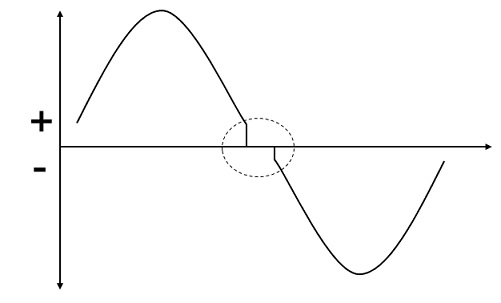
Figure 1 shows a graph of distortion. It was difficult to inject the charge and discharge signals in the same way in the conventional circuits, which improved the distortion by controlling the BJT offset of the push-pull circuit. In this paper, to solve this problem, we designed and simulated a circuit that can control charge and discharge cycles with one offset at the same time. In addition, the AC current detection circuit for the improved circuit is designed together.
2. Theory
2.1 Electrochemical Impedance Spectroscopy (EIS)
At a high frequency, the internal impedance is measured after measuring the changes in amplitude and phase according to the response waveform generated by sequentially applying an alternating waveform up to a low frequency [3][4].
2.2 Theory of EIS
As the reactance changes according to the frequency, the impedance in the AC circuit is affected by the capacitor and inductance. Therefore, to understand these characteristics according to the frequency, it is necessary to express them in complex numbers in complex plane.
When a smalling alternating current (I) is injected into the battery, an alternating voltage (V) is generated. Depending on the value of the internal impedance, a phase difference(Ø, Phase Shift) occurs. Equation (1) shows the internal impedance [5][6].
| (1) |
[R : Real part, jX : Imaginary part, XL : Inductive reactance, 1/XC : Capacitive reactance]
3. System configuration
3.1 Conventional EIS system
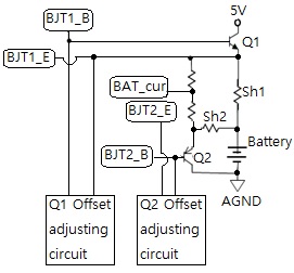
Figure 2 shows a modified version of the push-pull circuit as a conventional minute current injection circuit. An alternating current is applied to the battery via PNP and NPN BJT, and use Offset adjustment circuit to adjust the input waveform of Q1 and Q2 and design to be turn-on. This circuit is designed so that an alternating current can be measured through the resistances of Sh1 and Sh2 [3][5].
This method can minimizes the distortion, however, it is likely that the charge/discharge amount is not equally proportional(1:1). Therefore, the respective offset needs to be adjusted that affects the battery charge/discharge, Hence an improved circuit design that can minimize distortion is needed.
3.2 Proposed EIS System
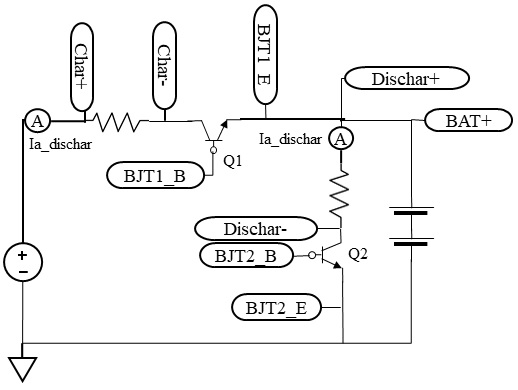
Figure 3 shows an AC voltage injection circuit in which a small charge/discharge alternating current of a battery is injected and a shunt resistor for measuring the current is connected. The AC voltage signal to be injected was reversely injected into the charging NPN and the room-specific NPN, and they were made to conduct in the same cycle so that the offset could be adjusted by one.
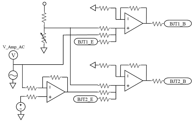
Figure 4 shows an offset adjustment circuit that makes charge/discharge the same at 1:1. The AC waveform input to the V_Amp_AC terminal is first converted into an AC signal and then inverted via Op-Amp. The half cycle of these two signals is higher than the turn-on voltage of each NPN shown in Figure 3. The offset voltage is adjusted according to the input, and a circuit that adds each emitter terminal voltage is added to make one offset adjustment. The amount of charge/discharge can be changed in the same cycle.
This method eliminates cross distortion by conducting AC voltage in the same period, and at the same time that enables 1:1 charge/discharge, and uses the conventional NPN and PNP BJT offset circuit circuits individually. This circuit was designed to eliminate the asymmetrical distortion.
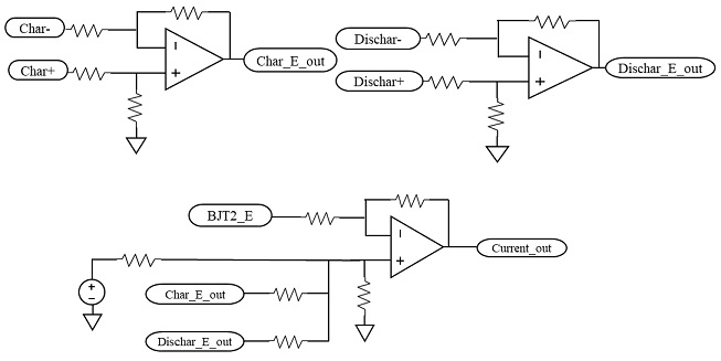
Figure 5 shows our proposed AC current detection circuit. In the case of conventional offset circuit, current detection resistor, a circuit is obtained which is obtained by alternating current from the battery voltage potential and adjusted to MCU voltage range. Therefore, we designed a circuit that converts AC wavefroms.
4. Simulation
4.1 Simulation of conventional circuit
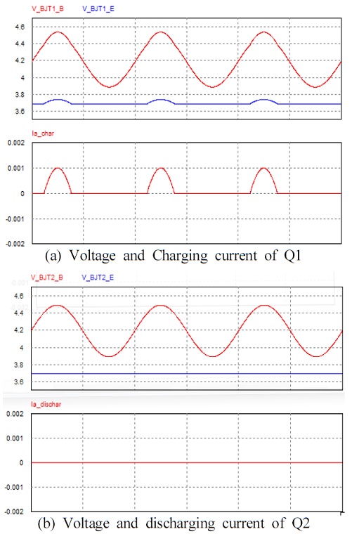
Figure 6 shows the current waveform of charge/discharge as the result of the simulation when two offset values were given 0 V and the current flowing through the BJT's base(B) and emitter(E) terminal voltages and the currents in each BJT. Figure 6 (a) shows the waveform during the charging of NPN BJT. The charging current appears because the BJT conducts only when the B terminal injection signal is 0.7V higher than the E terminal. Figure 6 (b) shows the waveform of the discharge part PNP BJT. BJT conducts only when the B-terminal injection signal is 0.7 V lower than the E terminal, but if the B-terminal injection signal is higher than the E terminal, no discharge current flows.
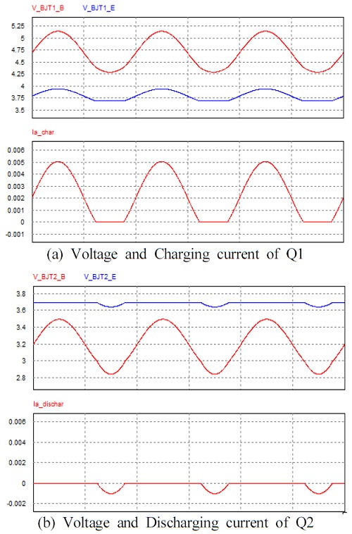
Figure 7 shows the simulation result of waveforms when the NPN BJT offset is 0.4 V and the PNP BJT offset is 1 V. Figure 7 (a) shows the waveform during NPN charging and the charging current cycle is greatly adjusted, and Figure 7 (b) is the waveform of the discharging unit PNP BJT when, the discharge current is reduced.
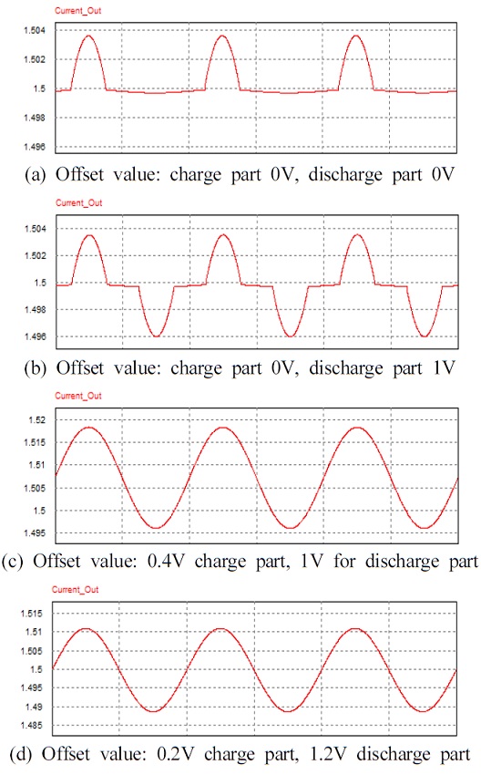
Figure 8 shows the waveform in which the current changes according to the charging and discharging unit and offset is detected. Figure 8 (a) when Offset was adjusted to the same value of 0V, the phenomenon that only the current of the charging part flows appears. Figure 8 (b) is current flows in both of the discharge but waveform distortion occurs. This is the case when both currents are full rotor and waveform distortion is displayed. In the case of Figure 8 (c), the waveform has no distortion, and charge/discharge currents do not flow in the same direction. As in the case of Figure 8 (d), the offset is injected such that it is 0.7 V from each emitter. In this case, there is no waveform distortion, and a current with the same amount of charge/discharge current can flow through the battery.
When offset is adjusted individually in the simulation result of the conventional circuit, the amount of charge/discharge is adjusted differently, and it is known that adjustment is necessary to adjust charge/discharge in the same cycle. If the two offsets are set to 1:1, there is no waveform distortion and the same charge/discharge amount can be set. However, in a board, it is difficult to set accurately because each is adjusted with a variable resistor.
4.2 Simulation of proposed system
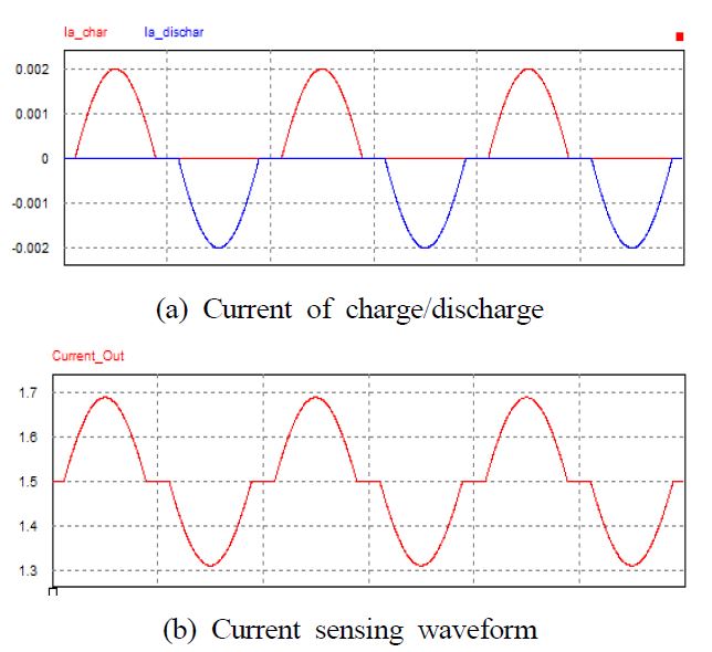
Figure 9 shows the charge/discharge current and current sensing waveforms when the charge/discharge amount was 50% or less with one offset in the proposed circuit. Figure 11 (a) is a charge current and discharge current waveform, which is adjusted by one offset circuit. Such that conduction cycle of BJT is the same for both charge/discharge, and it is insufficiently controlled and distortion occurs in the shape of the current sensing waveform in Figure 9 (b).
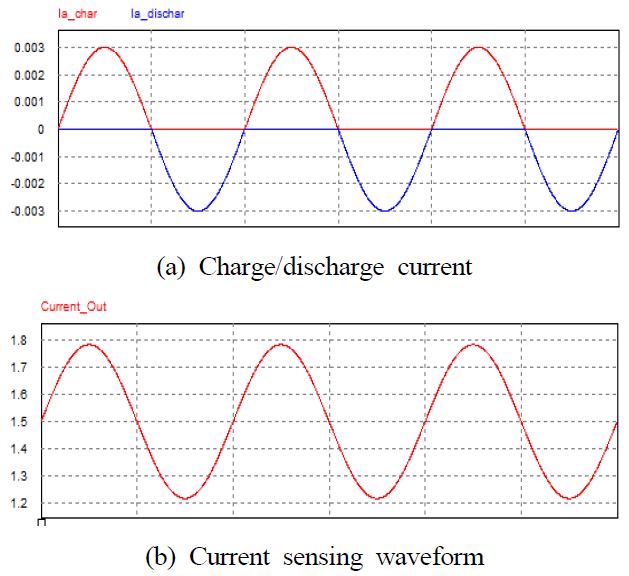
Figure 10 shows the charge/discharge current amount and current sensing waveform when the charge/discharge amounts was controlled to 50%. Figure 10 (a) shows that the cycles of charge and discharge are the same, and only 50% of the cycles flow current. Figure 10 (b) was confirmed that the amount of charge and discharge can be controlled in the same manner without distortion occurring as in the current detection waveform.
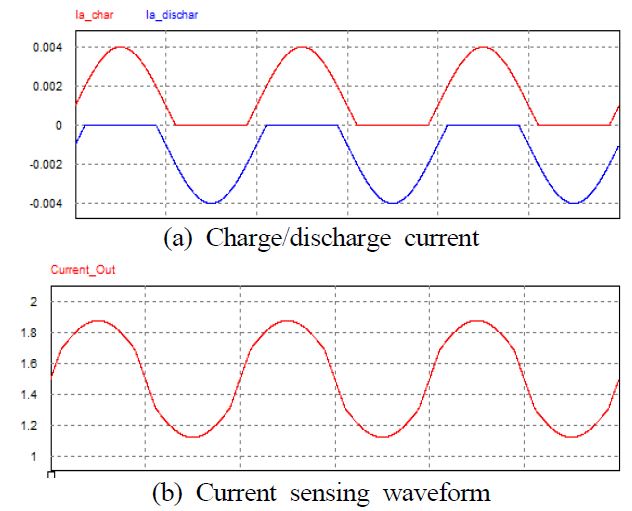
Figure 11 (a) shows the discharge current amount and current sensing waveform when the charge/discharge amounts were adjusted to be 50% or more. The amount of charge/discharge are the same, and the current flows continuously. However, as shown in the waveform Figure 11 (b), the sine wave has a distortion in the section where charge/discharge occur simultaneously. Through the simulation results using the proposed circuit, even if the offset is incorrectly set, the charge/discharge cycles are injected equally.
The existing circuit uses a variable resistor that raises the sine wave for NPN and a variable resistor that lowers the sine wave for PNP, changing the waveform and sending the charge/discharge waveforms respectively. The conduction size is determined by each variable resistor, and it is difficult to find an exactly 1: 1 matching interval.
The proposed circuit uses two NPN BJTs of the same size, and are conducted and superposed at the same time. It is possible to measure the internal impedance with a zero base without affecting the discharge.
4.3 Current measurement circuit
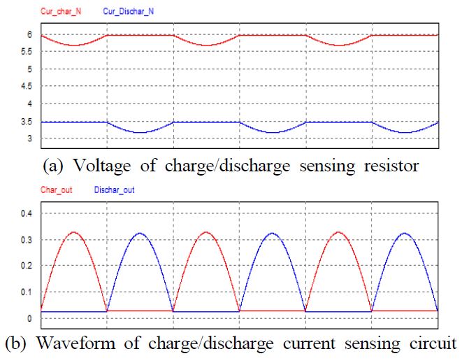
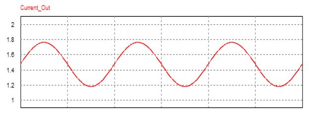
Figure 12 shows a waveform in which the voltage across the shunt resistor is detected to measure the current injected into the proposed EIS circuit. As both NPN BJTs are used for the charge/discharge circuit, the charge/discharge current is displayed in the same direction while the potential waveform is different as shown in Figure 12 (a). The current waveform is shown in Figure 12 (b).
Figure 13 is a circuit that is composed as shown in Figure 5 to output to the MCU in the form of alternating current. It allows you to adjust the offset within 1.5 V to maintain the waveforms within the 0 to 3 V of the MCU.
5. Conclusion
This study describeds an offset control circuit that can performed charge/discharge adjustment in the same cycle. This is an improvement over the previously proposed electrochemical impedance spectroscopy (EIS). A current sensing circuit suitable for the proposed circuit was designed and simulated to verify its validity.
As a result of simulating the possibility of applying the improved circuit proposed in this paper, the following conclusions were obtained.
- 1) When using the existing two offset circuits that minimize distortion generated in EIS equipment, adjust the value so that the charge/discharge amount is matched 1: 1 in the same cycle it was difficult. This point was improved, and a good sinusoidal charge/discharge AC signal having the same cycle as that of one offset circuit and having no distortion could be obtained.
- 2) Adjusting the point to eliminate cross distortion to make AC voltage conduct in the same cycle through the proposed circuit, at the same time, charge/discharge amount can be 1:1, for, each offset circuit of conventional NPN and PNP BJT circuit It was confirmed that it was possible to eliminate the amount of asymmetric distortion caused by the individual use.
- 3) The proposed equipment for minimizing distortion is easy to grasp the graph of fuel cell at a glance. It is expected to contribute to the safety of electric vehicles and electric propulsion ships.
Acknowledgments
Following are results of a study on the “Leaders in Industry-university Cooperation +” Project, supported by the Ministry of Education and National Research Foundation of Korea.
Author Contributions
Conceptualization, T. H. Song and S. G. Lee; Methodology, T. H. Song; Software, H. S. Yang; Validation, H. S. Yang; Formal Analysis, T. H. Song; Investigation, T. H. Song; Data Curation, J. W. Han; Writing—Original Draft Preparation, T. H. Song; Writing—Review & Editing, S. G. Lee; Visualization, T. H. Song; Supervision, S. G. Lee; Project Administration, S. G. Lee; Funding Acquisition, S. G. Lee;
References
- J. O. Park and S. Y. Kim, “Technology trends in ship electric propulsion systems,” The Korean Institute of Power Electronics, vol. 19, no. 3, pp. 31-37, 2014 (in Korean).
-
S. M. Kim, “Review of international regulations on greenhouse gas emissions from international shipping,” Environmental Law and Policy, vol. 23, pp. 141-172, 2019 (in Korean).
[https://doi.org/10.18215/elvlp.23..201909.141]

-
T. H. Song, J. L. Choi, H. S. Yang, Y. S. Kim, and S. G. Lee, “An improved battery impedance measurement module for electric propulsion ships and a study of battery characteristics,” Journal of the Korean Society of Marine Engineering, vol. 43, no. 2, 108-113, 2019 (in Korean).
[https://doi.org/10.5916/jkosme.2019.43.2.108]

-
T. H. Song, H. S. Yang, Y. S. Kim, and S. G. Lee, “Investigation of the lifespan characteristics of a rapid charge/discharge battery using the inverter level discharge method,” Journal of the korean Society of Marine Engineering, vol. 42, no. 7, pp. 615-619, 2018 (in Korean).
[https://doi.org/10.5916/jkosme.2018.42.7.615]

- T. H. Song, The study on the charge cycle for optimization of battery pulse charging, M.S. Dissertation, Department of Electrical and Electronic Engineering Graduate School of Korea Maritime and Ocean University, Korea, 2019 (in Korean).
- J. L. Choi, Study on Electrochemical Impedance Spectroscopy Equipment for Checking State of Battery, M.S. Dissertation, Department of Electrical and Electronic Engineering, Graduate School of KoreaMaritime and Ocean University, Korea, 2018 (in Korean).

