Suppression of silicon clusters using a grid mesh under DC bias
Copyright © The Korean Society of Marine Engineering
This is an Open Access article distributed under the terms of the Creative Commons Attribution Non-Commercial License (http://creativecommons.org/licenses/by-nc/3.0), which permits unrestricted non-commercial use, distribution, and reproduction in any medium, provided the original work is properly cited.
Abstract
Si clusters generated during the plasma chemical vapor deposition (CVD) process have a great influence on the qual ity of the fabricated films. In particular, in hydrogenated amorphous silicon thin films (a-Si:H) used for thin film solar cells, Si clusters are mainly responsible for light-induced degradation. In this study, we investigated the amount of clusters incorporated into thin films using a quartz crystal microbalance (QCM) and specially designed cluster eliminating filters, and investigated the effect of the DC grid mesh in preventing cluster incorporation. Experimental results showed that as the applied voltage of the grid mesh, which is placed between the electrode and the QCM, decreased, the number of clusters incorporated into the film decreased. This is due to the electrostatic force from the grid mesh bias, and this method is expected to contribute to the fab rication of high-quality thin films by preventing Si cluster incorporation.
Keywords:
Cluster, Amorphous silicon, Plasma CVD, Light-induced degradation1. Introduction
Plasma-enhanced chemical vapor deposition (PECVD) is employed to deposit various thin film materials in vacuum using activated radicals and ions in an excited plasma state. In particular, hydrogenated amorphous silicon (a-Si:H) films prepared by PECVD have attracted much attention in recent years due to their potential application as photovoltaic materials. However, there are several technical issues related to these devices, one of which is the fabrication of high-quality thin films while maintaining a high deposition rate. Although several research groups have reported stabilized cell efficiency over 10% in single junction, the deposition rate of less than 2 Å/s is too low for commercial application [1]-[3]. To achieve a high deposition rate, a high generation rate of the film precursors is required. The main species contributing to the film deposition are SiH3 radicals, but the highly ordered silane molecules, SinHm, are inevitably incorporated into the films during film growth [4]. The fraction of highly ordered silane molecules markedly affects the film quality. Thus, the analyses of the each radical and high ordered silane are very important.
To suppress such degradation of a-Si:H films, we have de veloped a multi-hollow discharge plasma CVD method, in which cluster incorporation can be significantly reduced in the upstream region due to the high gas flow velocity to drive clusters toward the downstream region[5]-[7]. By using this method, we successfully deposited a-Si:H films with a low sta bilized defect density of 4.7 × 1015 cm-3 at a high deposition rate of 3.0 nm/s [8]. The a-Si:H films show high stability against light exposure.
In this study, we focused on a method to suppress the in corporation of highly ordered Si clusters during film growth by applying a DC voltage to the grid mesh placed between the cathode electrode and the substrate. A specially designed QCM (quartz crystal microbalance) is used to observe the amount of Si clusters contributing to the deposition [9].
2. Experimental Method
The experimental setup consisted of a multi-hollow electro de as a remote plasma source, a grid mesh for setting the ex perimental conditions, and a QCM for measuring the accumu lated mass discharged from the plasma. Experiments were car ried out at a working pressure of 66.5 Pa and a 60MHz AC voltage with 40Vpp.
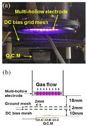
Silane was used as the process gas, and the flow rate wasmaintained at 30 sccm. The process gas injected into thechamber passed through the multi-hollow power electrode andflowed out to the exhaust gas treatment system. During theflow of the process gas, plasma was generated inside theholes, as shown in Figure 1 (a). The various radicals generated in the plasma underwent primary and secondary reactions and passed through the grid mesh located below the power electrode. The radical flux passing through the grid mesh, that is, the radicals contributing to the film growth, were measured in the specially designed QCM.
The QCM consisted of three channels (Figure 1 (b)). First, the SiH3 radicals, which are the main deposition species, were measured in Ch. A together with the Si clusters.
Next, in Ch. B, only the SiH3 radicals were measured with out the clusters. This was realized by installing a cluster elimi nating filter above the QCM sensor. Clusters with a short life time resulting from the high sticking probability were removed by the filter, and thus did not pass through the filter. On the other hand, SiH3 radicals with long life time resulting from the low sticking probability reached the QCM sensor without be ing trapped by the filter. In this experiment, the temperature of the quartz sensors was maintained at 373 K. On the other hand, the QCM was affected not only by the mass change on the quartz crystal sensor, but also by the substrate temperature and chamber pressure. Therefore, we installed Ch. C as a ref erence sensor to measure the influence of temperature and pressure by blocking the top of the sensor.
3. Results and Discussion
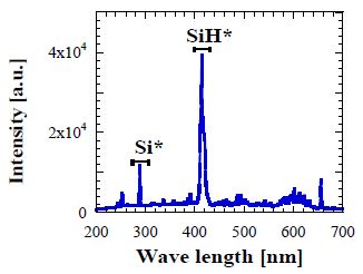
Optical emission spectroscopy (OES) analysis was recorded to determine the radical species emitted from the electrode holes, and their plasma electron temperature. Figure 2 shows the typical optical emission spectra obtained from plasma gen erated by silane discharge. Kampas and Griffith [10] demon strated that SiH* radicals are produced by one-electron impact dissociation, and Drevillon et al. [11] reported that Si*(288nm) and SiH*(414nm) species are generated from the primary colli sion of one electron with the silane molecules. Therefore, the optical emission intensity ratio Si*/SiH* would give in forma tion about the slope of the high-energy tail and can be used as a measure of electron temperature. Thus, if Si*/SiH* has a small value, the electron-energy distribution function (EEDF) becomes steep. Based on this information, we investigated the change in the plasma state depending on the applied bias change.
Figure 3 shows the OES data and oscilloscope information for the bias change during experiments, for determining the plasma state. The intensity of SiH* in Figure 3 (a) is reported to be proportional to the deposition rate of the thin film [12]. This is because the SiH* intensity is proportional to the rate of radical generation due to electron collision dissociation of SiH4. As shown in Figure 3 (a), the intensity of SiH* remained almost constant with the grid bias change. The Si*/SiH* value represents the high-energy tail of the EEDF, as des cribed above, which represents the electron temperature. The Si*/SiH* value remained almost constant with a change in the bias change, as shown in the Figure 3 (b). The electron tem perature is related to the formation of Si clusters in the plas ma; at high electron temperatures, highly reactive Si, SiH, and SiH2 species are easily generated in the plasma. The results in dicated that the cluster generation rate is constant with the grid mesh bias. Namely, both the SiH* intensity and Si*/SiH* intensity ratio remained unaffected by the grid mesh bias, and did not modify the radical density and cluster density during plasma discharge.
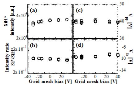
SiH* OES intensity (a), Si*/SiH* OES intensity ratio (b), Vpp (c) and Vdc (d) as a function of the grid mesh bias
Figure 3 (c) shows the results of peak-to-peak voltage (Vpp) measurement obtained using the oscilloscope. The Vpp valve was almost constant with bias change. The Vpp value is related to variation of the plasma potential. It was also confirmed that this did not change with the bias applied to the grid mesh out side the multi-hollow electrode. The Vdc voltage in Figure 3 (d) represents the sheath DC voltage applied to the powered electrode. This DC voltage difference was due to the differ ence in the flux of the electrons and ions reaching the electrode. In other words, it means that there is a potential dif ference between the surface of powered electrode and the bulk plasma. Thus, an electrostatic force and an ion drag force were generated in this region by such a potential difference. These forces were in balance, and the negatively charged clus ters floated at the end of the sheath. Therefore, the results de picted in Figure 3 (d) means that the generated clusters are trapped in the sheath and the forces on clusters are constant without change.
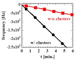
Figure 4 shows the frequency shift of the QCM due to dep osition with (w/) and without (w/o) the Si clusters. According to the Sauerbrey equation [13], the change in resonance frequ ency is inversely proportional to the mass change of the films deposited on the quartz sensor. For the frequency shift without clusters, the deposition rate decreased due to the installation of the cluster eliminating filter above the quartz sensor. Si clus ters with a high sticking probability were adsorbed on the fil ter surface without passing through the filters, while SiH3 radi cals with a low sticking probability reached the quartz sensor surface through the filters and contributed to the mass increase [14]. Thus, the main contribution of the w/o cluster in Figure 4 was thought to be due to SiH3 with a long lifetime. On the other hand, the w/ clusters is the mass increase including the contribution of SiH3 radicals together with the Si clusters. Using this method, we could briefly discuss the effect of the grid mesh bias on the deposition rate with and without clusters.
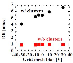
Figure 5 shows the deposition rate calculated using the fre quency shift of the QCM. Clusters in the plasma tend to be negatively charged due to the large cross sectional area and low velocity [15][16]. When the grid mesh potential is lower than the bulk plasma potential, the electrostatic force acts from the grid mesh toward the bulk plasma, and thus, it becomes difficult for the negatively charged clusters to pass through the grid mesh. This expectation is consistent with the experimental results in Figure 5. The number of w/ clusters decreased with a decrease in the bias of the grid mesh. These results indica ted that the negatively charged clusters could not pass through the mesh due to the electrostatic force. On the other hand, the number of w/o clusters remained constant because the SiH3 radicals mostly contributed to frequency shifting. Since the SiH3 radical had a smaller cross-sectional area and higher ve locity than the clusters, it could easily pass through the mesh without being negatively charged.
4. Conclusions
We investigated the effect of the mesh on the Si cluster in corporation through a specially designed QCM. When the grid mesh bias was lower than the plasma potential, the negatively charged clusters could not pass through the grid mesh due to the electrostatic force. Therefore, such plasma modification would be useful for preventing cluster incorporation in the fabrication of high-quality thin films.
Acknowledgments
This work was supported by Research Fund, Mokpo National Maritime University Industry-Academic Cooperation Foundation.
References
- P. Boeuf, Ph. Belenguer, and T. Hbid, “Plasma par ticle interactions”, Plasma Sources Science and Technology, vol. 3, p407-417, (1994).
-
D. M. Tanenbaum, A. L. Laracuente, and A. Gallagher, “Nanoparticle deposition in hydrogenated amorphous silicon films during rf plasma deposition”, Applied Physics Letters, vol. 68(no. 12), p1705-1707, (1996).
[https://doi.org/10.1063/1.115912]

- M. Shiratani, S. Maeda, K. Koga, and Y. Watanabe, “Effects of Gas Temperature Gradient, Pulse Discharge Modulation, and Hydrogen Dilution on Particle Growth in Silane RF Discharges”, Japanes Journal of Applied Physics, vol. 39(no. 1), p287-293.
-
S. Nunomura, I. Yoshida, and M. Kondo, “Time -dependent gas phase kinetics in a hydrogen diluted silane plasma”, Applied Physics Letter, vol. 94(no. 7), p071502, (2009).
[https://doi.org/10.1063/1.3086312]

-
K. Koga, N. Kaguchi, M. Shiratani, and Y. Watanabe, “Correlation between volume fraction of clusters incorporated into a-Si:H films and hydrogen content associated with Si–H2 bonds in the films”, Journal of Vacuum Science & Technology A, vol. 22(no. 4), p1536-1539, (2004).
[https://doi.org/10.1116/1.1763905]

-
K. Koga, T. Inoue, K. Bando, S. Iwashita, M. Shiratani, and Y. Watanabe, “Highly stable a-Si:H films deposited by using multi-hollow plasma chemical vapor deposition”, Japanese Journal of Applied Physics, vol. 44(no. 46-49), pL1430-L1432, (2005).
[https://doi.org/10.1143/jjap.44.l1430]

-
Y. Kim, K. Hatozaki, Y. Hashimoto, G. Uchida, K. Kamataki, N. Itagaki, H. Seo, K. Koga, and M. Shiratani, “High amount cluster incorporation in initial Si film deposition by SiH4 plasma chemical vapor deposition”, Japanese Journal of Applied Physics, vol. 52(no. 1S), p01AD01, (2013).
[https://doi.org/10.7567/jjap.52.01ad01]

-
W. M. Nakamura, H. Matsuzaki, H. Sato, Y. Kawashima, K. Koga, and M. Shiratani, “High rate deposition of highly stable a-Si:H films using multi-hollow discharges for thin films solar cells”, Surface Coatings Technology, vol. 205, pS241-S245, (2010).
[https://doi.org/10.1016/j.surfcoat.2010.07.081]

-
K. Koga, N. Kaguchi, K. Bando, and M. Shiratani, “Cluster-eliminating filter for depositing cluster-free a-Si:H films by plasma chemical vapor deposition”, Review of Scientific Instruments, vol. 76(no. 11), p113501, (2005).
[https://doi.org/10.1063/1.2126572]

-
H. Jia, J, K. Saha, N. Ohse, and H. Shirai, “High-rate synthesis of microcrystalline silicon films using high-density SiH4/H2 microwave plasma”, Thin Solid Films, vol. 515(no. 17), p6713-6720, (2007).
[https://doi.org/10.1016/j.tsf.2007.01.055]

-
G. Sauerbrey, “Verwendung von Schwingquarzen zur Wägung dünner Schichten und zur Mikrowägung”, Zeitschrift Für Physik, vol. 155(no. 2), p206-222, (1959).
[https://doi.org/10.1007/bf01337937]

-
J. Perrin, M. Shiratani, P. Kae-Nune, H. Videlot, J. Jolly, and J. Guillon, “Surface reaction probabilities and kinetics of H, SiH3, Si2H5, CH3, and C2H5 during deposition of a-Si:H and a-C:H from H2, SiH4, and CH4 discharges”, Journal of Vacuum Science & Technology A, vol. 166(no. 1), p278-289, (1998).
[https://doi.org/10.1116/1.580983]

-
Y. Watanabe, M. Shiratani, and K. Koga, “Clustering phenomena in low-pressure reactive plasmas. Basis and applications”, Pure Applied Chemistry, vol. 74(no. 3), p483-487, (2002).
[https://doi.org/10.1351/pac200274030483]

-
Y. Watanabe, “Formation and behaviour of nano/micro-particles in low pressure plasmas”, Journal of Physics D: Applied Physics, vol. 39(no. 19), pR329-R361, (2006).
[https://doi.org/10.1088/0022-3727/39/19/r01]

-
F. J. Kampas, and R. W. Griffith, “Optical emission spectroscopy: Toward the identification of species in the plasma deposition of hydrogenated amorphous silicon alloys”, Solar Cells, vol. 2(no. 4), p385-400, (1980).
[https://doi.org/10.1016/0379-6787(80)90014-9]

-
B. Drevillon, J. Hue, A. Lloret, J. Perrin, G. de Rosny, and J. P. M. Schmitt, “Silane dissociation mechanisms and thin film formation in a low pressure multipole dc discharge”, Applied physics letters, vol. 37(no. 7), p646-648, (1980).
[https://doi.org/10.1063/1.92008]


